HDI PCB & High Interconnect PCB Manufacturing
What is a high density PCB board (HDI PC?
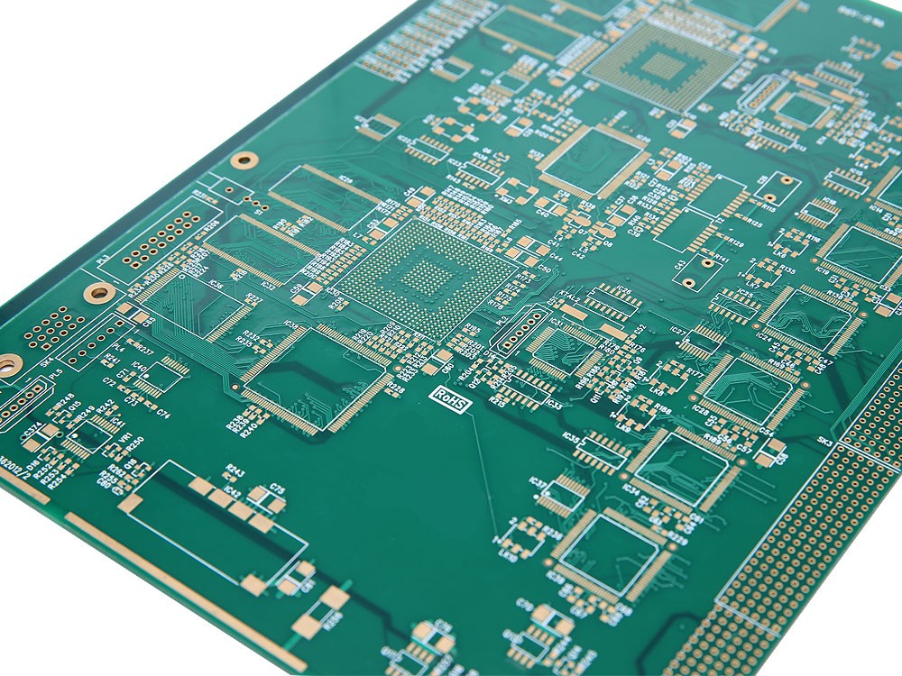
The HDI board is based on the traditional double panel as the core board, which is made by continuously accumulating. This circuit board made by a continuous layer is also called the Build-Up Multilayer (BUM). Compared with the traditional circuit board, the HDI circuit board has the advantages of "light, thin, short, small".
The electrical connection between HDI's plate layer is achieved by conductive pores, buried holes, and blind holes. Its structure is different from ordinary multi -layer circuit boards. A large number of blind holes are used in HDI boards. HDI PCB uses laser direct drilling, and standard PCB usually uses mechanical drilling, so the number of layers and high width ratio often decreases.
HDI includes the use of fine features or signal traces and spaces of 0.003” (75 µm) or less and laser-drilled blind or buried microvia technology. Microvias allow the use of micro-interconnects from one layer to another within a PCB utilizing a smaller pad diameter creating additional routing density or reducing form factor.
https://www.hitechpcba.com/hdi....-pcb-manufacturer-hi