In today's technologically advanced world, silicon wafers play a pivotal role in the production of electronic devices that have become an integral part of our daily lives. From smartphones and laptops to solar panels and advanced medical equipment, silicon wafers form the foundation of these cutting-edge technologies. This aims to take you on a fascinating journey into the world of Silicon Wafer Manufacturing, uncovering the intricate processes involved, and shedding light on the critical role they play in shaping our modern society.
The Basics of Silicon Wafers:
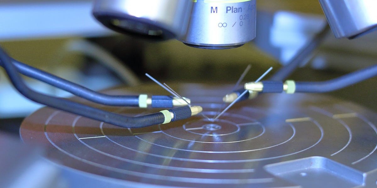
Before delving into the manufacturing process, let's familiarize ourselves with the fundamentals of silicon wafers. A silicon wafer is a thin, disc-shaped slice of crystalline silicon, typically extracted from a cylindrical ingot through a process known as slicing. Silicon, a widely abundant element, possesses remarkable semiconductor properties that make it an ideal material for electronic devices. These wafers serve as the canvases on which integrated circuits (ICs), also known as microchips, are created.
Properties of Silicon Wafers
Silicon wafers are characterized by several critical properties that determine their quality and usability. These include:
Diameter: Silicon wafers come in various sizes, commonly ranging from 2 to 12 inches in diameter. Larger wafers provide higher productivity and improved cost efficiency.
Orientation: Silicon wafers can have different crystal orientations, with the (100) and (111) planes being the most common. The orientation affects the electrical properties of the resulting integrated circuits.
Thickness: The thickness of silicon wafers is typically around 200-1000 micrometers, depending on the intended application. Thinner wafers are often used for more advanced and delicate devices.
Dopants: To modify the electrical characteristics of silicon, minute amounts of impurities called dopants are introduced during the manufacturing process. Common dopants include boron, phosphorus, and arsenic.
Silicon Wafer Manufacturing Process:
The production of silicon wafers involves a series of complex and precise steps. Let's explore the manufacturing process in detail:
· Silicon Ingot Growth
The journey of a silicon wafer begins with the growth of a silicon ingot through a process called Czochralski (CZ) crystal pulling. In this method, high-purity polycrystalline silicon is melted in a quartz crucible, and a seed crystal is dipped into the molten silicon. As the seed crystal is slowly withdrawn and rotated, a single crystal ingot is formed. This ingot serves as the source material for slicing into wafers.
· Wafer Slicing
Once the silicon ingot has been grown, it undergoes wafer slicing. In this stage, the ingot is cut into thin wafers using a precision cutting machine equipped with a diamond-edged saw. The slicing process generates a considerable amount of waste material, known as the "kerf," which is recycled to minimize material loss.
· Wafer Grinding
Following wafer slicing, the wafers undergo a grinding process to remove any surface damage caused during slicing. Precision grinding machines equipped with diamond wheels are used to reduce the wafer thickness to the desired level. This step requires careful control to ensure a uniform thickness across all wafers.
· Etching and Cleaning
After grinding, the wafers are subjected to a series of etching and cleaning steps to remove any impurities and contaminants. This involves immersing the wafers in chemical solutions that selectively etch away the surface layers and cleanse the wafers thoroughly. The cleaning process is crucial to ensure the wafers are free from particles and defects that could impact the performance of the final devices.
· Thermal Processing
Thermal processing, including oxidation and diffusion, is a vital step in silicon wafer manufacturing. Oxidation involves exposing the wafers to high temperatures in an oxygen-rich environment, forming a thin layer of silicon dioxide on the wafer surface. This layer serves as an insulating material in electronic devices. Diffusion, on the other hand, involves introducing dopants into the silicon lattice, altering its electrical properties as desired.
· Photolithography and Patterning
Photolithography is a key technique used to define the intricate patterns and features of the integrated circuits on silicon wafers. A photosensitive material called a photoresist, is deposited onto the wafer surface. Next, a photomask containing the desired circuit pattern is aligned and exposed to ultraviolet light, transferring the pattern onto the photoresist. The exposed areas of the resist are then chemically removed, leaving behind the patterned resist.
· Etching and Deposition
The patterned resist serves as a protective layer during subsequent etching and deposition processes. Etching selectively removes the unprotected areas of the silicon dioxide or silicon, creating the desired features on the wafer. Deposition techniques, such as chemical vapor deposition (CVD) or physical vapor deposition (PVD), are used to add layers of materials, such as metals or dielectrics, onto the wafer surface.
· Backend Processes
Once the desired circuitry is defined on the silicon wafer, a range of backend processes takes place. These processes include metallization, where conductive metals are deposited and patterned to form interconnects, and passivation, which involves coating the wafer with insulating materials to protect the delicate circuits. Backend processes also include dicing the wafer into individual chips and packaging them into final electronic devices.
Advancements in Silicon Wafer Manufacturing:
Over the years, silicon wafer manufacturing has witnessed significant advancements, driven by the constant demand for smaller, faster, and more powerful electronic devices. Some notable advancements include:
· Larger Wafer Sizes
The industry has steadily transitioned from smaller wafer sizes to larger ones. With the increasing popularity of 300mm (12-inch) wafers, manufacturers can achieve higher yields per wafer and reduce production costs. Larger wafer sizes also enable the integration of more devices on a single wafer, enhancing the performance and efficiency of electronic components.
· Thinner Wafers
As technology progresses, the demand for thinner wafers has grown. Thinner wafers offer advantages such as improved flexibility, enhanced heat dissipation, and reduced signal interference. Advanced manufacturing techniques, such as grinding and polishing, have made it possible to produce wafers with thicknesses below 100 micrometers, enabling the development of ultra-thin and flexible electronic devices.
· More Complex Circuitry
With the shrinking size of transistors and the advent of nanoscale technologies, Silicon Wafer Manufacturing has pushed the boundaries of creating more complex and intricate circuitry. This has been made possible through advancements in photolithography, such as multiple patterning and extreme ultraviolet (EUV) lithography, allowing for the creation of smaller features and higher transistor densities on the wafers.
· Advanced Materials and Processes
To meet the demands of emerging technologies, researchers and manufacturers are exploring new materials and processes. For example, silicon-on-insulator (SOI) wafers, where a thin layer of silicon is separated from the substrate by an insulating layer, offer improved performance and power efficiency. Additionally, innovative deposition techniques, such as atomic layer deposition (ALD), enable the precise deposition of ultra-thin films, enhancing the performance of integrated circuits.
Conclusion:
Silicon wafers, the unsung heroes of the electronics industry, have revolutionized the way we live, communicate, and interact with the world around us. The intricate process of silicon wafer manufacturing, from ingot growth to backend processes, showcases the meticulous craftsmanship and cutting-edge technologies involved in producing these essential building blocks of modern technology. With ongoing advancements and innovations, silicon wafer manufacturing continues to pave the way for smaller, faster, and more powerful electronic devices that shape our future. So, the next time you hold a smartphone or marvel at the wonders of modern technology, remember the silent contribution of silicon wafers in making it all possible.