In the world of semiconductor testing, precision and efficiency are paramount. As electronic devices become smaller and more complex, the need for advanced testing methods becomes increasingly crucial. One such innovation that has gained significant attention in recent years is the solder bump vertical probe card. This cutting-edge technology has revolutionized the way semiconductor testing is conducted, offering unparalleled accuracy and reliability. We will explore the intricacies of Solder Bump Vertical Probe Cards, their advantages, and the impact they have had on the semiconductor industry.
What is Solder Bump Vertical Probe Cards?
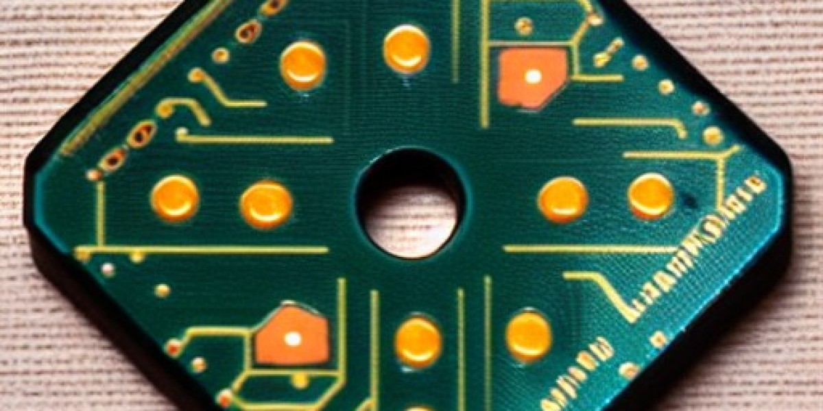
Solder bump vertical probe cards, also known as vertical probe cards or VPCs, are sophisticated testing tools used in the semiconductor industry. These cards consist of an array of tiny vertical probes that make contact with the solder bumps on a semiconductor wafer or package. The solder bumps serve as contact points for electrical testing and signal transmission.
How Do They Work?
The working principle of solder bump vertical and probe cards revolves around the use of vertically aligned probes. The probes are designed to be precisely aligned with the solder bumps on the semiconductor device under test. When the card is pressed onto the device, the probes make contact with the solder bumps, establishing an electrical connection. This connection allows for the transmission of test signals to the device and the measurement of various electrical parameters.
Advantages of Solder Bump Vertical Probe Cards:
Solder bump vertical probe cards offer several advantages over traditional testing methods. Let's take a closer look at some of the key benefits:
· Enhanced Accuracy
One of the primary advantages of solder bump and vertical probe cards is their exceptional accuracy. The vertical alignment of the probes ensures precise and reliable contact with the solder bumps, minimizing the risk of false readings or incomplete connections. This level of accuracy is particularly crucial in high-density semiconductor devices where even the slightest misalignment can lead to significant testing errors.
· Increased Test Speed
Speed is another area where solder bump vertical probe cards excel. The vertical probe design allows for simultaneous testing of multiple solder bumps, significantly reducing the overall test time. With conventional probe cards, testing each solder bump individually can be a time-consuming process, especially in complex integrated circuits. The enhanced test speed offered by vertical probe cards translates into improved productivity and faster time-to-market for semiconductor manufacturers.
· Cost Efficiency
Solder bump vertical probe cards also bring cost efficiency to the semiconductor testing process. By reducing test time and increasing throughput, manufacturers can optimize their resources and lower overall testing costs. Additionally, the high accuracy of vertical probe cards minimizes the need for retesting and rework, further reducing expenses. Over time, these cost savings can have a substantial impact on the profitability of semiconductor manufacturers.
· Extended Lifespan
Traditional probe cards often suffer from wear and tear due to repetitive contact with semiconductor devices. The vertical probe design of solder bump vertical and probe cards helps mitigate this issue. Since the probes make vertical contact with the solder bumps instead of sliding across the surface, the wear on the probes is significantly reduced. This extended lifespan of the probe cards leads to reduced maintenance and replacement costs for semiconductor manufacturers.
· Compatibility with Advanced Packaging Techniques
The semiconductor industry has seen a rapid evolution in packaging techniques, with a shift towards advanced packaging such as flip-chip and 3D IC. Solder bump and vertical probe cards are well-suited to handle these advanced packaging technologies. The vertical alignment of the probes enables seamless testing of solder bumps in various package types, ensuring compatibility with the latest semiconductor designs. This adaptability is crucial in keeping pace with the ever-changing landscape of semiconductor packaging.
Impact on the Semiconductor Industry:
The introduction of solder bump vertical probe cards has had a profound impact on the semiconductor industry. Here are a few notable effects:
· Improved Quality Control
With their high accuracy and reliability, solder bump vertical and probe cards have significantly improved quality control in semiconductor manufacturing. The precise testing provided by these cards helps identify and rectify defects at an early stage, minimizing the chances of faulty devices reaching the market. This enhanced quality control has bolstered consumer confidence in electronic products, leading to increased customer satisfaction and brand reputation for semiconductor manufacturers.
· Accelerated Time-to-Market
Time-to-market is a critical factor in the semiconductor industry, where competition is fierce. Solder bump vertical probe cards, by reducing testing time and increasing throughput, have contributed to faster product development cycles. The ability to quickly and accurately test semiconductor devices enables manufacturers to bring their products to market sooner, gaining a competitive edge and capturing market share ahead of their competitors.
· Facilitating Advanced Semiconductor Designs
As semiconductor designs continue to push the boundaries of innovation, testing methods must keep pace. Solder bump vertical probe cards have played a vital role in enabling advanced semiconductor designs, including those utilizing flip-chip and 3D IC technologies. The compatibility and adaptability of vertical probe cards have facilitated the development and testing of cutting-edge semiconductor devices, opening up new possibilities for the industry.
· Driving Research and Development
The introduction of solder bump and bumps vertical probe cards has sparked increased research and development in the field of semiconductor testing. Manufacturers and testing equipment suppliers are investing resources to enhance the capabilities of vertical Probe Cards, exploring new materials and designs to further improve accuracy, speed, and reliability. This ongoing research and development drive is instrumental in driving the semiconductor industry forward and pushing the boundaries of what is possible.
Conclusion:
Solder bump vertical probe cards have emerged as a game-changer in the field of semiconductor testing. With their enhanced accuracy, increased test speed, cost efficiency, extended lifespan, and compatibility with advanced packaging techniques, these cards have revolutionized the way semiconductor devices are tested. The impact of probe cards on the semiconductor industry is far-reaching, enabling improved quality control, accelerating time-to-market, facilitating advanced designs, and driving research and development. As technology continues to advance, we can expect further innovations in the field of semiconductor testing, with solder vertical probe cards at the forefront of these developments.