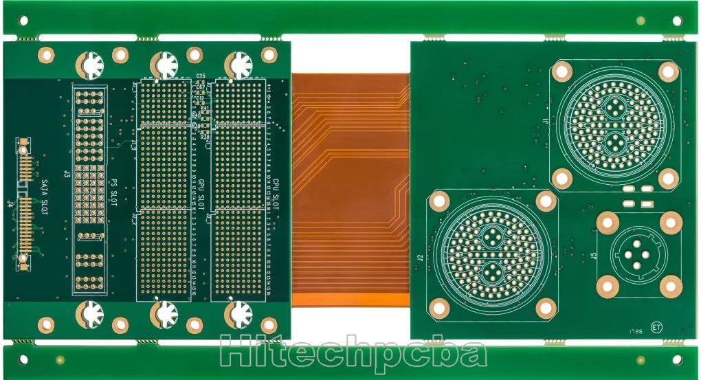
As the name implies, a Rigid-Flex PCB is a hybrid of a Flex PCB and a Rigid PCB. The combination of the two types of boards utilises the benefits each one provides, integrating the versatility of the flexible board with the robustness of the rigid board. Rigid-flex printed circuit boards are used in more complex mechanical designs, eliminating flexible cables and wiring and replacing it with integrated circuits.
Rigid-Flex PCBs, by definition, are a combination of rigid part(s) joined by interconnecting flex areas where the flex material is used across the entire PCB area.
The rigid parts are where there is no bending requirement. Again, PTHs take connections from layer to layer as required. Rigid-flex may also employ other technologies as required eg. HDI. Unlike the cost-effective flex PCBs, Rigid-Flex PCBs can be a bit more costly due to their intricate design.
Rigid-flex PCB design can be used to eliminate or greatly reduce requirements for bulky and costly cable harnesses, in turn taking out costs and reducing assembly time. Like the pure flexible PCBs, a high volume of rigid-flex PCBs are used in aviation and space applications – and also in automotive and test equipment.
The flexible layers of a Rigid-Flex PCB are buried within the board and penetrate through the rigid sections of the PCB.
The trend to miniaturization in electronics continues. Integrated circuit board solutions are becoming more and more popular as a means of efficiently utilizing the even smaller casing volume in all three dimensions.
Benefits of Rigid Flex PCB
Space requirements can be minimized by applying 3D
By removing the need for connectors and cables between the individual rigid parts the board size and overall system weight can be reduced.
By maximizing space, there is often a lower count in parts.
Less solder joints assure higher connection reliability.
Handling during assembly is easier in comparison with flexible boards.
Simplified PCB assembly processes.
Integrated ZIF contacts provide simple modular interfaces to the system environment.
Test conditions are simplified. A complete test prior to installation becomes possible.
Logistical and assembly costs are significantly reduced with flex-rigid boards.
It is possible to increase the complexity of mechanical designs, which also improves the degree of freedom for optimized housing solutions.
Rigid Flex PCB Fabrication Applications
Rigid flexible PCBs offer a wide array of applications, ranging from military weaponry and aerospace systems to cell phones and digital cameras. Increasingly, rigid flex board fabrication has been used in medical devices such as pacemakers for their space and weight reduction capabilities. The same advantages for rigid flex PCB usage can be applied to military weaponry and weapon control systems
In consumer products, rigid flex doesn't just maximize space and weight but greatly improves reliability, eliminating many needs for solder joints and delicate, fragile wiring that are prone to connection issues. These are just some examples, but rigid flex PCBs can be used to benefit nearly all advanced electrical applications including testing equipment, tools and automobiles.
Available structures for rigid flex PCB
There are numerous, different structures available. The more common ones are defined below:
Traditional rigid flex construction (IPC-6013 type 4) Multilayer rigid and flexible circuit combination containing three or more layers with plated through holes.
Asymmetrical rigid flex construction, where the FPC is situated on the outer layer of the rigid construction. Containing three or more layers with plated through holes.
Multilayer rigid flex construction with buried / blind via (microvia) as part of the rigid construction. 2 layers of microvia are achievable. Construction may also include two rigid structures as part of a homogeneous build.
The Disadvantage and Advantage of Rigid-Flex PCB
Rigid-flex PCB has many production processes with the characteristic of superior difficulty in production and high defect rate. Its biggest disadvantage is that the price is more expensive than flex PCB or rigid PCB and long production cycle. Another disadvantage is that both SMT and furnaces may need to use carrier to support the flex PCB which virtually increases the SMT cost.
One of the key features of rigid-flex PCB is the thin profile and changeable shape, making it an ideal solution for ultra -thin and ultra -light packaging. Although the rigid flex PCB may be more expensive in design and manufacturing, they do have many advantages and can solve many problems in traditional hardboard technology.
1. Small Size and Flexible Shape
The rigid- flex PCB is easier to install more components in smaller space, because they can change the shape according to a specific contour. This technology will reduce the size and weight of the final product and the overall system cost. At the same time, the compact shape of rigid flex PCB makes it the best choice for fine lines and high -density circuits in HDI technology.
2. Customized for Different Applications
Rigid-flex PCB has various packages, which can be customized for the application of many industries such as aerospace, military, medical equipment and consumer electronics. They can customize the size and shape to adapt to the shell design and 3D design, which provides designers with more possibilities to meet different requirements in specific applications.
3. Better Mechanical Stability
The stability of the rigid board and the flexibility of the flexible board form the stable structure of the entire packaging, while retaining the reliability and flexibility required for small space installation.
4. Good Performance in Harsh Environments
Rigid-flex PCB has high resistance and high vibration capacity, so they can work normally in a high -stress environment. There are fewer cables and connectors used in rigid-flexible PCB, which also reduces security risks and maintenance in future use.
5. Easy to Manufacture and Test
The rigid-flex PCB requires a small number of inter connect and related components/parts. It helps simplify the assembly operation, making rigid –flex PCB easier to assemble and test. Rigid-flex PCB is very suitable for PCB prototypes.
In addition to the above advantages, other common advantages of rigid-flex PCB also include high circuit density, good heat dissipation and good chemical resistance. In a word, rigid-flex PCB combines all the advantages of rigid PCB and flex PCB, and at the same time make up for the shortcomings. This PCB is the best solution to design reliable and powerful circuits for smart wearable devices and other industries.
Rigid-flex PCB board, it is a circuit board that combines flexible and rigid circuit board technology in the application. Most rigid-flex boards are composed of multiple layers of flexible circuit boards, which are attached to one or more rigid boards from the outside and/or from the inside, depending on the design of the application. The flexible substrate is designed to be in a constant deflection state, and is usually formed as a deflection curve during rigid flex pcb manufacturing or assembly.
Hitech rigid flex pcb manufacturing process
After the production of FPC flexible boards is completed, the production of Hitech rigid flex pcb boards can be completed through the following processes.
1. Punching
Drill holes on FR4 and PP film, and the design on the alignment hole is not the same as the general through hole. After the punching is completed, browning is required.
2. Riveting
Laminate copper clad laminates, PP adhesives, and FPC circuit boards and place them neatly. The original old process is to laminate and pressing step by step, but it is a waste of time. After many attempts, we found that the stacking process can be completed once.
3. Laminate
This is a relatively complete step in the production of rigid-flex pcb board. Most of the materials are integrated for the first time. First, the bottom layer is copper clad laminate and PP film, above are the FPC flexible board produced in the previous process, and a PP film is placed on the FPC flexible board, then place the last layer of copper clad laminate. All materials to be laminated are placed in order and pressed together.
4. Trimming
That is to remove the part of the circuit board where there is no circuit at the edge of the circuit board currently and in the future. Afterwards, it is necessary to measure whether the material has excessive expansion and contraction. Because the PI used in the production of flexible boards is also expansion and contraction, this has a very large impact on the production of circuit boards.
5. Drilling
This step is the first step to turn on the entire circuit board, and the production parameters should be produced according to the design parameters.
6. Desmear
First, remove the scum generated by the drilling of the circuit board, and then use plasma cleaning to clean the through holes and the board surface.
7. Immersion copper
This step is the process of electroplating through holes, also known as hole metallization. Realize through-hole power conduction.
8. Plate plating
Partially electroplating copper on the upper surface of the electroplating hole makes the copper thickness above the through hole exceed a certain height of the copper clad board surface.
9. Outer dry film positive film production
The same as the production process of the anti-corrosion dry film of the FPC board, the circuit to be etched on the copper clad board is made. After the development is completed, check the circuit.
10. Graphic plating
After the initial copper sinking, pattern electroplating is performed, and the current time and copper plating wire are used according to the design requirements to reach a certain electroplating area.
11. Alkaline etching
12. Print solder mask
This step has the same effect as the FPC board protective film. We see that the PCB rigid board is generally green. This step is generally called green oil printing. After the printing is completed, the inspection is carried out.
13. Open the cover
Cover opening, which is the area where the FPC board is located, but the area not needed by the rigid board is laser cut to expose the FPC board.
14. Curing
It is also a baking process.
15. Surface treatment
Generally, at this time, a rigid-flex PCB board has been manufactured, and only the metallization treatment is required on the surface of the circuit board, which can play a role in preventing wear and oxidation. Generally, this process is to soak the circuit board in a chemical solution, and the metal elements in the solution are densely distributed on the circuit board circuit.
16. Characters printing
The positions of the parts to be assembled and some basic product information are printed on the rigid-flex board in the form of characters.
17. Test
This is a process of checking whether the circuit board is qualified. The test items are tested for electrical properties according to customer requirements. The tests generally include impedance test, open and short circuit test and so on.
18. Final inspection
19. Packaging and shipping
There are many ways to package circuit boards. Generally, Hitech use packaging bags to separate them, and then use a vacuum packaging machine to vacuum package the rigid-flex PCB boards .
The advantages of rigid-flex PCB board
1). It can effectively save the space on the circuit board and eliminate the use of connectors
Because the FPCB and rigid pcb board has been combined, the space that originally needed to use the connector can be saved. For some circuit boards with high-density requirements, less connectors will be better. In this way, it also saves the cost of parts using the connectors. In addition, the space between the two boards can be made tighter by eliminating the need for connectors.
2). The signal transmission distance is shortened and the speed is increased, which can effectively improve the reliability
The traditional signal transmission through the connector is “circuit board→connector→flexible pcb board→connector→circuit board”, while the signal transmission of the rigid-flex PCB board is reduced to “rigid circuit board→flexible pcb board→rigid circuit board”, signal transmission distance between different media is shortened, and the problem of signal transmission attenuation between different media is also reduced. Generally, the circuit on the PCB board is made of copper, while the contact terminal of the connector is gold-plated, and the solder pin is fully tin-plated. Moreover, solder paste is required to be soldered on the circuit board, and the signal transmission between different media will inevitably be attenuated. If you switch to a rigid-flex PCB board, these media will become less, and the signal transmission ability can be relatively improved. For some products that require higher signal accuracy, it helps to improve their reliability.
3). Simplify product assembly and save assembly time
The use of a rigid-flex PCB board can reduce the man-hours for SMT parts, because the number of connectors is reduced. It also reduces the man-hours for assembly of the whole equipment, because it eliminates the assembly action of inserting the FPC board into the connector. It also reduces the cost of parts management and inventory, because the required parts is reduced, so the management cost becomes less.
The disadvantages of rigid-flex PCB boards
The biggest disadvantage of the rigid-flex PCB board is that the price of “rigid-flex PCB board” is more expensive, and it may be nearly double the original price of pure “FPC board + rigid PCB board”, but if the price of the connector and processing cost is deducted, the price may tend to be the same, and the detailed cost may have to be actuated to have a clearer outline.
Another disadvantage is that it may need to use a carrier to support the part of the FPC board for both the production and the furnace, which invisibly increases the assembly cost of the SMT.
Applications of rigid-flex PCB boards
The rigid-flex PCB boards provide a wide range of applications from smart devices to mobile phones and digital cameras. Rigid-flex board manufacturing has been increasingly used in medical devices such as pacemakers to reduce their space and weight. The use of rigid flexible PCB has the same advantages and can be applied to intelligent control systems.
FAQs on Rigid-Flex PCBs at Hi-Tech Circuits
1. Can Hitech Circuits customize Rigid-Flex PCBs for specific applications? Absolutely! Hitech Circuits specializes in customizing Rigid-Flex PCBs to meet specific design requirements and applications. Our team works closely with clients to ensure the final product meets their exact specifications.
2. Are there any limitations to the design of Rigid-Flex PCBs? While Rigid-Flex PCBs offer great flexibility and versatility, there are some limitations in terms of maximum size and complexity due to manufacturing constraints. However, our team is experienced in overcoming these challenges to meet client needs.
3. What is the typical lead time for a Rigid-Flex PCB project? Lead times can vary depending on the complexity of the design and the specific requirements of the project. Generally, it ranges from a few weeks to several months. We prioritize efficient production while maintaining high-quality standards.
4. How does Hitech Circuits ensure the quality of their Rigid-Flex PCBs? Quality assurance is integral to our process. We conduct rigorous testing and inspection at every stage of production, from raw materials to the final product, ensuring that each PCB meets our high standards and client expectations.
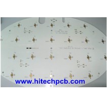
Metal Core PCB Metal Core PCB, MCPCB Manufacturing Service
What is aMetal Core PCB?
Metal core aluminum PCB is an aluminum-based copper clad laminate with good heat dissipation function. Generally, the single layer aluminum-based PCB is composed of a three-layer structure, which is a circuit layer (copper foil), an insulating layer and a metal base layer. Also used for high-end use is designed as a double sided and multilayer aluminum PCB.
A metal core PCB is a special PCB having a metallic base layer. This base layer is usually made of aluminum or copper. As it contains a metallic layer, it is named Metal Core PCB (MCPC.
An aluminum PCB is a printed circuit board that contains a thin layer of conductive dielectric material. They are also called aluminum cladding, aluminum base, MCPCB (metal clad printed circuit board), IMS (insulated metal substrate), thermal conductive PCB, etc. Aluminum PCBs were developed in the 1970s, and soon their applications increased sharply. The first application is their use in amplifying hybrid integrated circuits. They are being used on a large scale, so we must understand aluminum PCB and its importance.
The metallic layer present in the metal core PCB does many wonders along with the dielectric layers. These PCBs are far better than FR-4 PCBs in terms of bearing thermal and pressure stresses. They are suitable for extreme conditions and high heat-dissipating components. Therefore, it has solved many issues that were faced in other PCB substrates. Metal core PCBs have tons of benefits, but all of them come at an additional cost.
What is IMS Circuit board ?
Insulated Metal Substrate (IMS)
The use of IMS circuit boards for simple single-layer circuits is a special but very effective method of heat dissipation for components across circuit boards. These generally consist of aluminium supports, insulation layers and copper foil. The base materials are available in different design versions.
Aluminum pcb Applications:
LED technology: Illuminated signs, displays and lighting
Automotive industry: LED headlights, engine control and power steering
Power electronics: DC power supply, inverters and engine control
Switches and semi-conductor relays
Aluminum pcb Manufacturing process
The metal core PCB fabrication process is ①Grinding plate (500# brush)→②Washing→③Passivation→④Washing×3→⑤Blow-drying→⑥Drying. Grinding plate: Grinding the iron surface only, grinding the plate according to FR4 parameters.
Metal core PCBs must follow a particular process due to the presence of the metal layer in the stackup. If the board is a single-layer board with no layer transitions back to the metal plate, then the standard FR4 dielectrics can be used, where the dielectric layer is pressed and bonded to the metal plate.
For multilayer dielectric stackups, the metal core must first be drilled to allow for a layer transition without creating a short circuit. First, slightly larger holes are drilled into the metal layer, and the holes are plugged with an insulating gel. This gel is cured and hardened, allowing it to be plated with copper, just like a standard via. The rest of the stackup is pressed and bonded with the metal layer, and through-holes are drilled through the stackup, followed by plating and cleaning.
The first board must check the circuit without scratches, black tin surface, other defects, and uniform wear marks.
Why Choose us for Metal core PCB ?
Competitive Cost for PCB Manufacturing
We offer high-quality customized PCB Boards with reasonable cost and the best service because we know the cost is significant to a product’s success. We have cost control for each process to provide reasonable PCB costs for our customers.
The reason why we can provide you with low-priced PCB manufacturing services is that we have a very complete supply chain management system and maintain a perfect and solid cooperative relationship with suppliers, and through mass procurement and mass production to reduce costs to a greater extent to customers so that you enjoy lower prices than the same industry, higher than the quality of the same industry.
Free DFM PCB Design Checking
We have a professional engineering team to provide complete engineering support for customers. Free DFM helps to save cost and reduce potential problems during PCB (printed circuit board) manufacturing.
Ten professional PCB engineers with over 20 years of PCB experience, with rich experience in various industry standards and process quality requirements, provide customers with optimized design PCB solutions at the design-in stage.
Advanced Automatic Production Equipment
Advanced PCB manufacturing and PCB assembly Production Equipment, Skilled Technical Workers are the Guarantee of Product Quality.
We Guarantee to Provide Reliable Products Based on Advanced Manufacturing Testing Equipments, Well-known Raw Materials and Comprehensive Management Systems.
Exquisite PCB Fabrication and PCBA Manufacture Capacity
The following is a list of some of our current manufacturing capacity, but not all. In addition, thanks to the fact that we are a private enterprise, in order to meet the needs of customers, we are constantly upgrading our own production equipment and production process.
Please trust us. We can provide a one-stop complete service from PCB prototyping to PCB assembly. Please feel free to contact us to find out if we can manufacture your PCB, give us a chance to work with you and give yourself a chance to find a more suitable PCB supplier.
Just send us your Gerber file, our professional sales staff will provide you with a fast and accurate PCB quote.
Looking for the best metal core PCBs? Hitech Circuits offers superior aluminum and copper PCB solutions for LED lighting, automotive, telecom, and other demanding applications. With over 10 years of experience, we provide optimized thermal management, increased power density, and maximum durability.
As the best metal core PCB manufacturer, our product withstands extreme temperatures to keep components cool even at high power levels. Get the most out of your designs with flexible, high-quality, custom-fabricated metal-core PCBs to your specifications.
Trust the metal core PCB experts at Hitech Circuits for unbeatable thermal performance and value.
About Our Metal Core PCB
Metal core printed circuit boards (PCBs) are vital in applications requiring high heat dissipation. Their enhanced thermal efficiency enables greater power densities while keeping components cool for increased durability. Metal core PCBs also facilitate driving components harder and shaping/forming the circuits. This makes them ideal solutions for the LED lighting industry.
Benefits of Using Our PCBs in LED Lighting
The lighting sector has evolved tremendously with the help of advanced PCB technologies for superior lumen output. Cost-effective aluminum-backed PCBs in particular, enable the creation of affordable high-performance lighting set-ups. Several advantages make PCBs perfectly suited for LED lighting:
Optimized Thermal Management
Metal core PCBs like aluminum-backed ones offer the best balance between thermal performance and cost. The metal core enables dissipation of heat more efficiently, increasing component life.
Higher Power Densities
By keeping components cooler even at higher power inputs, metal core PCBs facilitate greater power densities within smaller hardware footprints.
Driving Components Harder
The improved cooling capacity provided by metal core PCBs also allows modules and components to be driven at higher operating limits for increased durability and performance.
Customizable Shapes
Our metal core PCBs can be shaped, drilled, or formed as per application requirements, adding great flexibility. Contact our metal core PCB manufacturer and share your requirements.
Structure of Metal Core PCBs
Aluminum base copper clad laminate, the raw material for metal core PCBs, has three key layers:
Circuit Layer
This layer with copper thickness from 1-10oz is equivalent to the copper layer in regular PCB laminates.Dielectric Insulation Layer
With a thickness ranging from 0.003” to 0.006”, this special material provides electrical insulation between the circuit and the metal base. It has low thermal resistance for heat transfer and UL certification for safety.
Metal Base Layer
Usually made of aluminum or copper, this thick metal layer enables heat dissipation from the PCB to the surroundings.
Key Characteristics
The main characteristics of metal core PCBs are
Greatly enhanced thermal management through improved heat spreading and dissipation
Optimal balance of thermal performance vs. cost
Withstands high temperatures and power levels reliably
Types of Metal Core PCBs
Some common varieties of metal core PCBs offered are:
Single Layer Aluminum Base
These PCBs have 3mm aluminum base thickness, 1 oz copper layer, and special thermal dielectric material with thermal conductivity of 3W/mK.
Double-Layer Aluminum PCB Boards
These allow greater circuit complexity with aluminum thickness from 0.8mm to 3.8mm. Additional coatings like solder or scratch resistance can be applied.
Bergquist Brand Metal Core PCB
Offering Bergquist aluminum metal core PCB with exceptional 2.4W/mk thermal conductivity for demanding applications.
High Current LED Boards
Special high thermal conductivity aluminum PCBs designed specifically for high-power LED lighting setups.
Customized Metal Core PCBs
Fully customized aluminum or copper PCBs fabricated per specific application requirements
Call Hitech Circuits For Your Project!
As the best metal core PCB manufacturer, we design and develop our products with the ability to handle high power densities. Our metal core PCBs are significant for LED lighting and other heat-generating electronics applications. With various options available, designers now have abundant choices to create efficient and durable systems in compact form factors at optimized costs.
Browse our products and call our experts at +86-755-29970700 to make an informed decision. We will gladly help you with your needs.
FAQs
1. What types of applications use metal-core PCBs?
LED lighting, automotive electronics, telecom infrastructure, and other high-power electronics utilize metal-core PCBs for their thermal performance. They are ideal for applications that generate significant heat.
2. What metals are used in the base layer of metal core PCBs?
Aluminum and copper are the most common base layer metals used. Aluminum provides the best balance of thermal conductivity and cost. Copper offers the highest performance for the most demanding applications.
3. What are some key design considerations for metal-core PCBs?
Consider the required power levels, operating temperatures, component spacing, board thickness, dielectric material, base metal choice, weight limitations, and special thermal needs. Share your requirements with the PCB manufacturer.
4. Can metal core PCBs be customized?
Yes, metal core PCBs can be fabricated in different shapes, with various drilling/routing patterns, edge treatments, coatings, and other customizations per specific design needs.
5. How can I get started with your metal core PCB fabrication services?
Contact our engineering team to discuss your project requirements. We will provide design recommendations, pricing, and manufacturing timelines to deliver high-quality custom metal core PCBs tailored to your application.
6. What are the lead times for prototype vs production metal core PCB orders?
Prototypes can be delivered in 2-4 days. Production lead times range from 2-4 weeks, depending on order quantity and customization. We can meet urgent delivery needs.
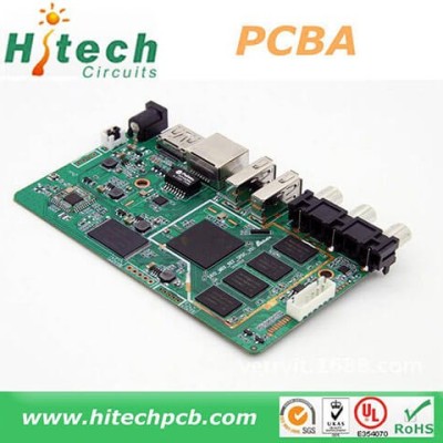
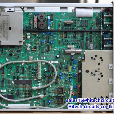
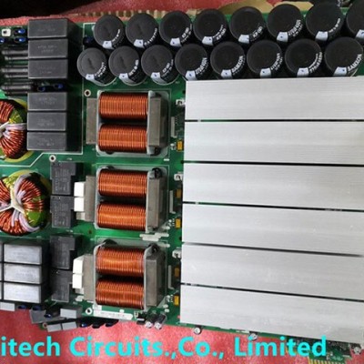
It’s the step in the manufacturing process in which you populate a blank board with the electronic components needed to make it into a functional printed circuit board. It’s these components that make a board into the circuit that enables an electronic product to function. PCB assembly typically takes place via one of two processes:
1. Surface-mount technology
SMT: SMT stands for “Surface Mount Technology“. The SMT components are very small sizes and comes in various packages like 0201, 0402, 0603, 1608 packages for resistors and capacitors. Similarly for Integrated circuits ICs we have SOIC, TSSOP, QFP and BGA.
The SMT components assembly is very difficult for human hands and can be time taking process so it is mostly done by automated pick and place machine.
2. Through-hole manufacturing
THT: THT stands for “Through hole Technology”. The components with leads and wires, like resistors, capacitors, inductors, PDIP ICs, transformers, transistors, IGBTs, MOSFETS are example.
The component has to be inserted on one side of PCB and pulled by leg on other side and cut the leg and solder it. The THT components assembly is usually done by hand soldering and is relatively easy.
Printed Circuit Board AssemblyTechniques
There are only two common PCBA techniques available for use by a PCB designer. The methods are:
**1. Automated PCB Assembly Techniques **
Generally, this technique employs the use of state of the art machines, which are fully automatic. For example, the surface mount components are worth positioning with the aid of an automated pick and place machine.
Again, reflow soldering is commonly for surface mount components usually done in a reflow oven. An automated solder stencil is also used to apply the solder paste on the PCB.
Finally, high tech inspection machines are used to confirm and check the quality of the PCBA. Some of which include: Automated optical inspection machine (AOI), X-ray inspection machines, etc.
Above all, due to the precise monitoring, control of soldering, no human input and versatile machines.
This technique ensures utmost efficiency, output consistencies, and limits defects.
2. Manual PCB Assembly Techniques
This method is favorite for use with through-hole parts, which needs manual placement on the board. Besides, with these through-hole parts, it’s advisable you use wave soldering. Note that in the through- hole assembly process, you need to place the components and electronics on the PCB.
After that, you use wave soldering to solder the leads. Typically, you will need an individual to insert a component into a marked PTH. Once done, transfer the PCB to the next station where the next person will be on standby tasked with fixing another part.
What are the Benefits of SMTPCB Assembly?
SMT assembly provides many benefits and some of them are as follows:
It can be used to incorporate small components.
In SMT, the components can be placed on both sides of the board.
It assures high component densities.
Fewer holes need to be drilled for surface mounting than through-hole.
It require low initial costs and time for setting up the mass production.
SMT is the simpler and faster-automated assembly when compared to through-hole.
Errors regarding the component placement can be easily rectified.
Surface mount PCBs feature strong joints, which can easily withstand vibrations.
What are the techniques used in Surface Mount Technology?
There are several techniques for the reflow process. After applying the solder paste or a flux mixture on the board and after placing the components, the boards are conveyed to a reflow soldering oven. The techniques used for reflowing soldering include infrared lamps, hot gas convection, fluorocarbon liquids with a high boiling point, and so on.
What are the different testing methods used in SMT PCB Assembly?
Hitech Circuits as the PCB assembly manufacturer, we perform the following testing and inspection to ensure the quality of surface mount PCBs.
Automated Optical Inspection (AOI): This is performed before and after the soldering to identify the component placement, presence, and solder quality.
X-ray Testing: In this type of testing, the operator relies on the X-ray images of the PCB to check the solder joints and lead-less components such as Quad Flat Packs and ball grid arrays, which are generally not visible to naked eyes.
In-Circuit Testing (ICT): This method is used to detect manufacturing defects by testing the electrical properties in the SMT Assembly.
What type of files or documents should I send for SMT PCB Assembly?
Gerber Files: The file contains all details of physical board layers including solder masks, copper layers, drill data, legends, and so on.
Bill of Materials (BOM): This contains information on the list of items needed for the PCB manufacturing and the instructions of manufacturing.
Pick and Place File: This file contains information on all components to be used in the PCB design and their rotation and X-Y coordinates.
The whole process ofPCB Assembly
1. Bare board loader machine
The first step in the PCB assembly is to arrange the bare boards on the rack, and the machine will automatically send the boards one by one into the SMT assembly line.
2. Printing solder paste
When PCB on the SMT production line, firstly, we have to print solder paste on it, and the solder paste will be printed on the pads of the PCB. These solder pastes will be melt and solder the electronic parts to the circuit board when it passes through the high-temperature reflow oven.
In addition, when testing new products, some people will use film board/adhesive cardboard instead of solder paste, which can increase the efficiency for adjusting the SMT machines.
3. Solder paste inspection machine(SPI)
Since the quality of solder paste printing is related to the quality of welding of subsequent parts, some SMT factories will use optical machine to check the quality of solder paste after printed the solder paste in order to ensure stable quality. If there any poorly printed solder paste board, we will wash off the solder paste on it and reprint, or remove the excess solder paste if there is redundant solder paste on it.
4. High speed SMT machine
Usually, we will put some small electronic parts (such as small resistors, capacitors, and inductors) to be printed on the circuit board first, and these parts will be slightly stuck by the solder paste just printed on the circuit board, so even if the speed of printing is very fast and the parts on the board will not fall away. But large parts are not suitable for use in such high speed SMT machines, which will slow down the speed of small parts assembly. And the parts will be shifted from the original position due to the rapid movement of the board.
5. Universal SMT machine
Universal SMT machine is also known as "slow machine", it will be assembled some large electronic components, such as BGA IC, connectors, etc., these parts need more accurate positions, so the alignment is very important. Use a camera to take a picture to confirm the position of the parts, so the speed is much slower than High speed SMT machine we taked before. Due to the size of the components here, not all of them are packed in tape and reel, and some may be packed in trays or tubes. But if you want the SMT machine to recognize the trays or tube-shaped packaging materials, you must configure an additional machine.
Generally, traditional SMT machines are using the principle of suction to move electronic parts, and in order to place the parts successfully, and there must be the flat surface on these electronic components for the suction nozzle of the SMT machine to absorb. However, for some electronic parts don’t have a flat surface for these machines, and it is necessary to order special nozzles for these special-shaped parts, or add a flat tape on the parts, or wear a flat cap for thees electronic parts.
6. Manual parts or visual inspection
After assembled all parts by the high speed SMT machine or Universal SMT machine and before going through the high-temperature reflow oven, and we will set up a visual inspection station here and to pick out the deviation parts or missing components boards etc., because we have to use a soldering iron to repair if there are still defectives boards after passing the high-temperature oven, which will affect the quality of the product and will also increase the cost. in addition, for some larger electronic parts or traditional DIP parts or some special reasons cannot be processed by the SMT machine before, they will be manually placed on pcb here.
7. Reflow oven
The purpose of reflow oven is to melt the solder paste and form a non-metallic compound on the component feet and the circuit board, that means to solder electronic components on the circuit board. The temperature rise and fall curves often affect the soldering quality of the entire circuit board. According to the characteristics of the solder materials, usually the reflow oven will set the preheating zone, soaking zone, reflow zone, and cooling zone to achieve the best soldering effect.
For example, the melting point for SAC305 solder paste with lead-free is about 217°C, which means that the temperature of the reflow oven must be higher than the melting points to remelt the solder paste. What's more, the maximum temperature in the reflow furnace should not exceed 250°C, otherwise many parts will be deformed or melted because they cannot withstand such a high temperature.
Basically, after the pcb passed through the reflow oven, the assembly for the entire circuit board is almost complete. If there are hand-soldered parts, we need to transfer to DIP process, and then we have to check the quality after reflow oven by QC department.
8. Automatic optical inspection(AOI)
The main purpose of setting up AOI is because some high density boards can’t be process the following ICT test, so we used AOI inspection to replace it. But even using AOI inspections, there still have the blind spots for such checking, for example, the solder pads under the components cannot be checked by AOI. At present, it can only check whether the parts have side standing issue, missing parts, displacement, polarity direction, solder bridges, lack of soldering etc., but cannot checking the BGA solderability, resistance value, capacitance value, inductance value and other components quality, so far AOI inspection can’t completely replace ICT test.
Therefore, there is still some risk if only AOI inspection is used to replace ICT testing, but ICT test is also not 100% make sure the good quality, we suggest these two ways can be combined with together to make sure the good quality.
9. PCB unloader machine
After the board is fully assembled, it will be retracted to the unloder machine, which has been designed to allow the SMT machine to automatically pick and place the board without damaging the quality for PCB.
10. Visual inspection for finished products
Normally there will be a visual inspection area in our SMT production line whether there is an AOI station or not, and it will help to check if there are any defectives after completed assembled the pcbs. If there is an AOI station, it can reduce the visual inspection worker on our SMT line, and to reduce the potential cost, and because it is still necessary to check some places that cannot be judged by AOI, many SMT factories will provide the mainly visual inspection templates at this station, which is convenient for visual inspection worker to inspect some key parts and polarity for components.
11. DIP process
DIP process is a very important process in the whole PCBA processing, and the processing quality will directly affect the functional for PCBA boards, so it is necessary to pay more attention to the DIP process. There are many preliminary preparations for DIP process. The basic process is to re-process the electronic components first, like to cut the extra pins for some DIP components, our staff received the components according to the BOM list, and will check whether the material part numbers and specifications are correct or not, and performs pre-production pre-processing according to the PCBA samples. The steps are: Use various related equipment (automatic capacitor pins cutting machine, jumper bending machine, diode and triode automatic forming machine, automatic belt forming machine and other machines) for processing.
12. ICT test
Printed Circuit board open/short circuit test (ICT, In-Circuit Test), The purpose of ICT test is mainly to test whether the components and circuits on the printed circuit board are open or short issues. It can also measure the basic characteristics of most components, such as resistance, capacitance, and inductance values to judge whether the functions of these parts are damaged, wrong parts or missing parts etc. after passing through the high-temperature reflow oven.
ICT test machines are divided into advanced and basic machines. The basic ICT test machines are generally called MDA (Manufacturing Defect Analyzer). It’s just to measure the basic characteristics of electronic components and judge open and short circuits issue we talked above.
In addition to all the functions of the basic ICT test machines, for advanced ICT test machine can also test the whole PCBA by using power, start to testing the PCBA boards by setting the program in the test machine. The advantage is that it can simulate the function of the printed circuit board under the actual power-on condition, this test can partly replace the following functional test machine (Function Test). But the cost for the test fixture of this advanced ICT test can probably buy a car, it’s too expensive and we suggest it can be used in mass production products.
13. PCBA function test
Functional testing is to make up for the ICT test, because ICT only tests the open and short circuits on the the PCBA board, and other functions such as BGA and other fuctions are not tested, so it is necessary to use a functional testing machine to test all functions on the whole PCBA board.
14. Cutting board (assembly board de-panel)
Normally, printed circuit boards will be produced in panel, and it will be assembled to increase the efficiency of SMT production. It means several single boards in one panel, such as two-in-one, four-in-one etc. After finished all the pcb assembly process, it needs to be cut into single boards, and for some printed circuit boards with only single boards also need to cut off some redundant board edges.
There are several ways to cut the printed circuit board. You can design the V-cut using the blade cutting machine (Scoring) or directly manually break off the board (not recommended). For more high density circuit boards, it will be used the professional splitting machine or the router to split the board without any damage the electronic components and printed circuit boards, but the cost and working hours will be a little longer.
Why Choose Hitech Circuits PCB Assembly Manufacturer for Your PCB Assembly Projects?
There are several PCB manufacturers specializing in PCB assemblyservices. However, Hitech Circuits PCB Assembly stands out owing to the following:
Assistance in Material Procurement:
Technically, in PCB assembly services, the quality of parts is the responsibility of the OEM; however, we ease your job by assisting you to make the right selection. We can help you procure all your parts of the same type own a single part number, thanks to our supply chain and vendor network as well as experience. This saves time and cost that goes in ordering single parts as you plan.
Testing procedures:
We are very focused on quality and thus implement stringent testing procedures at each stage of the assembly and after completion.
Fast Turnaround Times:
Our well-equipped facility and the right tools enable us to complete your requirements well before time, and without compromising on the quality or functioning of the PCBs. For simple designs we revert in 24 to 48 hours.
Cost Effectiveness:
While PCB assembly is a cost-effective alternative, we go a step further and assure that the parts you list are of a good quality and suitable for your requirement. Also, you can control the part flow and replenish them as needed. This eliminates the need to buy extra stock and store it.
Quick Quote:
We offer a quick quote based on your BOM. All you need is a detailed BOM, Gerber files, your application requirement sheet, and quantity.
We’re not one to stand still, which is why we use the latest equipment and the finest minds to create your PCB projects. We’re constantly keeping our finger on the pulse of the latest trends. And as a result, we know how to deliver the highest standards of PCB assembly to meet all your requirements.
Our dedicated, friendly customer service team also means that we support you every step of the way. Offering our expert guidance to ensure a complete PCB project that you’re happy with.
Hitechpcba is a wоrld-lеаding PCB Manufacturing & PCB Assembly company with more than 20 years experience in the electronics manufacturing industry. We focus on PCB Design, PCB Layout, Circuit board fabrication, Turnkey PCB assembly, and electronic parts sourcing services.
With mature supply chain, talented design team, advanced manufacturing techniques and quality control systems, Hitechpcba is able to provide one-stop electronics manufacturing services and solution for our customers to help them stand out in the marketplace.
We offer a full range of Electronic manufacturing services.
Är du säker på att du vill ta bort den här medlemmen från din familj?
Du har petat PCBAseembly_Hitech
Ny medlem har lagts till i din familjelista!
Beskär din avatar
Kommentaren har rapporterats.
Inlägget har lagts till på din tidslinje!
Du har nått din gräns på 5000 vänner!
Filstorleksfel: Filen överskrider den tillåtna gränsen (954 MB) och kan inte laddas upp.
Din video bearbetas. Vi meddelar dig när den är redo att visas.
Det går inte att ladda upp en fil: Den här filtypen stöds inte.
Vi har upptäckt en del barnförbjudet innehåll på bilden du laddade upp, därför har vi avvisat din uppladdningsprocess.
Dela inlägg i en grupp
Dela till en sida
Dela till användare
Ditt inlägg skickades, vi kommer att granska ditt innehåll snart.
För att ladda upp bilder, videor och ljudfiler måste du uppgradera till proffsmedlem. Uppgradera till PRO
Redigera erbjudande
Lägg till nivå
Ta bort din nivå
Är du säker på att du vill ta bort den här nivån?
Recensioner
För att sälja ditt innehåll och dina inlägg, börja med att skapa några paket. Intäktsgenerering
Betala med plånbok
Lägg till paket
Radera din adress
Är du säker på att du vill ta bort den här adressen?
Ta bort ditt paket för intäktsgenerering
Är du säker på att du vill ta bort det här paketet?
Säga upp
Är du säker på att du vill avsluta prenumerationen på den här användaren? Tänk på att du inte kommer att kunna se något av deras intäktsgenererade innehåll.